
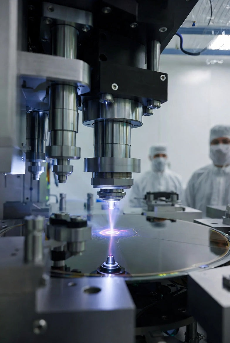
Precision Without Heat: How Ultrafast Lasers Are Transforming Semiconductor Processing
As semiconductor nodes shrink below 2nm and advanced packaging becomes increasingly complex, manufacturers face a growing challenge: how to machine, anneal, and modify materials with extreme precision without destroying delicate structures through heat. The solution increasingly lies in ultrafast lasers — femtosecond and picosecond systems that deliver energy faster than heat can spread.
These “cold ablation” tools are rapidly moving from niche research applications into mainstream semiconductor manufacturing, enabling cleaner cuts, better yields, and new process capabilities.
The Power of Ultrafast Pulses
Traditional lasers operate on nanosecond timescales, where heat diffusion causes unwanted side effects like melting, cracking, or damage to surrounding areas (known as the heat-affected zone, or HAZ). Ultrafast lasers, with pulse durations measured in femtoseconds (10⁻¹⁵ seconds) or picoseconds (10⁻¹² seconds), deposit energy so quickly that material is removed via multiphoton ionization and Coulomb explosion — essentially vaporizing atoms with minimal thermal transfer.
Key applications in 2025–2026 include:
- Wafer dicing and stealth dicing: Creating clean, chip-free edges on silicon, glass, and brittle materials without mechanical stress.
- Micro-via drilling and through-glass vias (TGVs): Essential for advanced 3D packaging and chiplet architectures.
- Laser annealing: Selective, localized dopant activation with ultra-low thermal budgets, improving performance in power semiconductors and advanced logic chips.
- Precision micromachining: Patterning redistribution layers, trimming resistors, and structuring low-k dielectrics without delamination.
Market Momentum and Industry Adoption
The ultrafast laser segment is experiencing strong growth. The broader laser micromachining machine market was valued at approximately $4.2 billion in 2025, with ultrafast systems holding the largest share (~42%) and projected to grow at nearly 9% CAGR through 2034. Major players such as Coherent, TRUMPF, IPG Photonics, and Jenoptik are expanding offerings tailored for semiconductor fabs.
In 2025–2026, companies like 3D-Micromac and Applied Materials have rolled out new selective laser annealing systems that deliver superior dopant activation while minimizing thermal impact on surrounding structures — critical for next-generation power devices and sensors.
Research institutions and consortia are also pushing boundaries. European projects have demonstrated laser-based transfer of 2D materials (like graphene) onto CMOS-compatible wafers, while academic teams continue to improve beam-shaping and process monitoring for higher throughput.
Why It Matters for the Industry
The rise of AI accelerators, high-bandwidth memory, and heterogeneous integration demands ever-more sophisticated packaging. Ultrafast lasers enable:
- Higher yields through damage-free processing
- Support for new materials (glass, sapphire, advanced dielectrics)
- Faster prototyping and repair capabilities
- Reduced reliance on slower, more hazardous chemical or mechanical processes
As the semiconductor industry races toward angstrom-scale features and denser 3D stacking, ultrafast laser technology is becoming a quiet but essential enabler — helping manufacturers maintain Moore’s Law momentum while controlling costs and improving reliability.
Looking Ahead
Industry observers expect continued convergence between ultrafast lasers and AI-driven process control, further optimizing parameters in real time. By the end of the decade, these tools could be as standard in advanced fabs as EUV lithography systems are today.
The laser isn’t just helping make better chips — it’s redefining what’s possible in semiconductor fabrication itself.