
Photonic Quantum Computing Enters Hardware Test & Validation Phase with New PsiQuantum Lab
PsiQuantum’s official opening of its Asia-Pacific Test & Validation Lab at Griffith University’s Nathan Campus on May 27, 2026, signals that photonic quantum computing has moved firmly into the engineering characterization and subsystem validation stage.
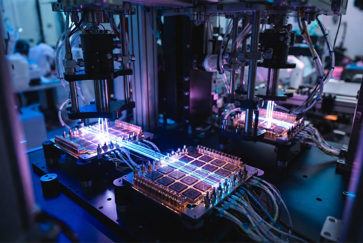
The lab, now fully constructed and operational, will focus on testing and qualifying photonic quantum components — including waveguides, single-photon sources, detectors, and optical switches — critical for scaling toward fault-tolerant, utility-scale systems.
From Roadmap to Real Infrastructure
This facility represents a concrete step beyond laboratory prototypes. Researchers and engineers at the site will conduct detailed characterization of photonic integrated circuits under conditions that simulate real-world manufacturing and deployment stresses. The lab supports PsiQuantum’s broader push to build a million-physical-qubit photonic quantum computer using silicon photonics fabrication techniques.
Simultaneously, PsiQuantum made its Construct fault-tolerant quantum computing (FTQC) software platform more widely available, giving external teams tools to design and simulate large-scale photonic circuits with realistic error correction.
For photonics engineers, this shift is highly recognizable: the emphasis is now on measurable metrics like insertion loss, photon indistinguishability, detector efficiency, and packaging reliability — the day-to-day parameters that determine whether a photonic platform can scale beyond a few hundred qubits.
Implications for Labs, Suppliers, and Optical Engineering
University groups and national laboratories working on quantum networking or hybrid systems will benefit from increased access to standardized photonic test data. The Griffith lab also strengthens workforce development in quantum photonics, an area where skilled optical engineers and laser technicians remain in short supply.
Photonics component suppliers (such as those providing ultra-low-loss waveguides, high-efficiency single-photon detectors, or precision alignment systems) should see clearer demand signals. Laser safety professionals and lab managers will need to prepare for expanded facilities handling high-power control lasers, cryogenic optical setups, and automated optical characterization equipment.
This development aligns with broader industry moves: tighter integration between photonic chip fabrication (e.g., through GlobalFoundries partnerships) and rigorous validation protocols that mirror semiconductor industry standards.
Practical Outlook for the Field
Photonic approaches have always promised advantages in room-temperature operation, networking compatibility, and manufacturability using existing semiconductor tools. The opening of dedicated test infrastructure like PsiQuantum’s Griffith lab indicates these advantages are now being stress-tested at scale.
For researchers writing proposals, hardware teams iterating on interconnects, and laboratory managers planning equipment budgets, the message is consistent: photonic quantum computing has entered the “build it and measure it” phase. The technical friction points — optical loss budgets, component yield, and system-level integration — are now front-and-center engineering challenges rather than distant theoretical ones.
This infrastructure build-out positions photonics as one of the more production-ready paths toward useful quantum systems in the coming years.